- 您现在的位置:买卖IC网 > Sheet目录362800 > EVAL-AD421EB (Analog Devices, Inc.) Loop-Powered 4 mA to 20 mA DAC
AD421
–
9
–
REV. C
The HC11 generates the requisite eight clock pulses with data
valid on the rising edges. After the MSBY is transmitted, the
least significant byte (LSBY) is loaded from memory and
transmitted in a similar fashion. To complete the transfer, the
LATCH pin is driven high when loading the complete 16-bit
word into the AD421.
AD421 TO MICROWIRE INTERFACE
The flexible serial interface of the AD421 is also compatible
with the National Semiconductor MICROWIRE interface. The
MICROWIRE interface is used in microcontrollers such as the
COP400 and COP800 series of processors. A generic interface
to use the MICROWIRE interface is shown in Figure 9. The
G1, SK, and SO pins of the MICROWIRE interface respec-
tively connect to the LATCH, CLOCK, and DATA IN pins of
the AD421.
SK
SO
CLOCK
DATA IN
LATCH
AD421*
MICROWIRE
* ADDITIONAL PINS OMITTED FOR CLARITY
Figure 9. AD421 to MICROWIRE Interface
G1
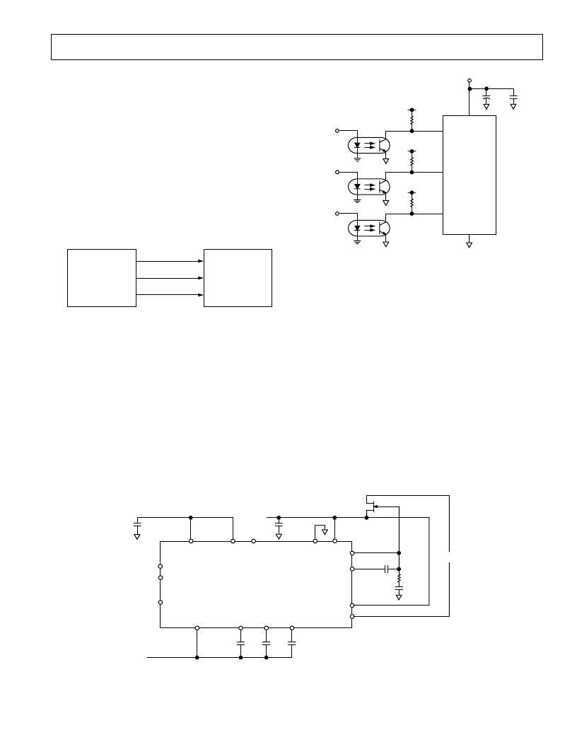
Opto-Isolated Interface
The AD421 has a versatile serial 3-wire serial interface making
it ideal for minimizing the number of control lines required for
isolation of the digital system from the control loop. In intrinsi-
cally safe applications or due to noise, safety requirements, or
distance, it may be necessary to isolate the AD421 from the
controller. This can easily be achieved by using opto-isolators.
Figure 10 shows an opto-isolated interface to the AD421 where
CLOCK, DATAIN and LATCH are driven from opto-couplers.
Be aware of signal inversion across the opto-couplers. If opto-
couplers with relatively slow rise and fall times are used, Schmitt
triggers may be required on the digital inputs to prevent errone-
ous data being presented to the DAC.
0.1 F
2.2 F
V
CC
10k
V
CC
10k
V
CC
10k
V
CC
CLOCK
LATCH
DATA IN
AD421*
COM
CLOCK
LATCH
DATA IN
V
CC
* ADDITIONAL PINS OMITTED FOR CLARITY
Figure 10. Opto-Isolated Interface
APPLICATIONS SECTION
Basic Operating Configuration
Figure 11 shows the basic connection diagram for the AD421
operating at 5 V. This circuit shows the minimum of external
components to operate the AD421. In the diagram, the AD421’s
regulator loop in conjunction with the DN25D pass transistor
provides the V
CC
voltage for the AD421 itself and for other
devices in the transmitter. The V
CC
pin should be well decou-
pled with a 2.2
μ
F capacitor to ensure regulator stability and to
absorb power glitches on the V
CC
line of the AD421 and other
devices in the system. If the AD421 is operated with V
CC
= 3 V,
the transfer function shifts negative. To correct for this a 16k
resistor connected between COM and LOOPRTN will approxi-
mately compensate for the V
CC
supply sensitivity in moving from
5 V to 3 V by adjusting the gain of the AD421.
C1
C2
C3
COM
COM TO EXTERNAL
CIRCUITRY
V
CC
LV
2.2 F
COM
V
CC
TO EXTERNAL
CIRCUITRY
DN25D
DRIVE
COMP
0.01 F
1k
1000pF
BOOST
LOOP RTN
V
LOOP
0.01 F
0.01 F
0.0033 F
LATCH
CLOCK
DATA
REF IN
REF OUT2
REF OUT1
4.7 F
COM
AD421
Figure 11. Basic Connection Diagram
发布紧急采购,3分钟左右您将得到回复。
相关PDF资料
Eval-AD5025EBZ
Fully Accurate 12-/14-/16-Bit VOUT DAC SPI Interface 2.7 V to 5.5 V in a TSSOP
Eval-AD5045EBZ
Fully Accurate 12-/14-/16-Bit VOUT DAC SPI Interface 2.7 V to 5.5 V in a TSSOP
Eval-AD5065EBZ
Fully Accurate 12-/14-/16-Bit VOUT DAC SPI Interface 2.7 V to 5.5 V in a TSSOP
EVAL-AD5066EBZ
Fully Accurate 16-Bit UnBuffered VOUT DAC SPI Interface 2.7 V to 5.5 V in a TSSOP
EVAL-AD5379EB
40-Channel, 14-Bit, Parallel and Serial Input, Bipolar Voltage-Output DAC
EVAL-AD5381EB
40-Channel, 3 V/5 V, Single-Supply, 12-Bit, Voltage Output DAC
EVAL-AD5382EB
32-Channel, 3 V/5 V, Single-Supply, 14-Bit, Voltage Output DAC
EVAL-AD5383EB
32-Channel, 3 V/5 V, Single-Supply, 12-Bit, Voltage Output DAC
相关代理商/技术参数
EVAL-AD5025EBZ
制造商:AD 制造商全称:Analog Devices 功能描述:Fully Accurate 12-/14-/16-Bit VOUT DAC SPI Interface 2.7 V to 5.5 V in a TSSOP
EVAL-AD5045EBZ
制造商:AD 制造商全称:Analog Devices 功能描述:Fully Accurate 12-/14-/16-Bit VOUT DAC SPI Interface 2.7 V to 5.5 V in a TSSOP
EVAL-AD5060EB
制造商:Analog Devices 功能描述:EVAL BD FOR AD506X DAC 14-/16BIT, SERL INPUT - Bulk
EVAL-AD5060EBZ
功能描述:BOARD EVAL FOR AD5060 RoHS:是 类别:编程器,开发系统 >> 评估板 - 数模转换器 (DAC) 系列:nanoDAC™ 产品培训模块:Lead (SnPb) Finish for COTS
Obsolescence Mitigation Program 标准包装:1 系列:- DAC 的数量:4 位数:12 采样率(每秒):- 数据接口:串行,SPI? 设置时间:3µs DAC 型:电流/电压 工作温度:-40°C ~ 85°C 已供物品:板 已用 IC / 零件:MAX5581
EVAL-AD5061EBZ
功能描述:BOARD EVALUATION AD5061 RoHS:是 类别:编程器,开发系统 >> 评估板 - 数模转换器 (DAC) 系列:nanoDAC™ 产品培训模块:Lead (SnPb) Finish for COTS
Obsolescence Mitigation Program 标准包装:1 系列:- DAC 的数量:4 位数:12 采样率(每秒):- 数据接口:串行,SPI? 设置时间:3µs DAC 型:电流/电压 工作温度:-40°C ~ 85°C 已供物品:板 已用 IC / 零件:MAX5581
EVAL-AD5062EB
制造商:Analog Devices 功能描述:EVAL BD FOR AD506X DAC 14-/16BIT, SERL INPUT - Bulk
EVAL-AD5062EBZ
功能描述:BOARD EVAL FOR AD5062 RoHS:是 类别:编程器,开发系统 >> 评估板 - 数模转换器 (DAC) 系列:nanoDAC™ 产品培训模块:Lead (SnPb) Finish for COTS
Obsolescence Mitigation Program 标准包装:1 系列:- DAC 的数量:4 位数:12 采样率(每秒):- 数据接口:串行,SPI? 设置时间:3µs DAC 型:电流/电压 工作温度:-40°C ~ 85°C 已供物品:板 已用 IC / 零件:MAX5581
EVAL-AD5063EB
制造商:Analog Devices 功能描述:Evaluation Board For 14-/16-Bit, Serial Input, Vout NanoDACs 制造商:Analog Devices 功能描述:EVAL BD FOR AD506X DAC 14-/16BIT, SERL INPUT - Bulk